Creating custom printed circuit boards has become increasingly accessible to hobbyists over the past decade, but traditional fabrication still takes days. For situations requiring ultra-rapid prototypes, a clever approach combines a standard 3D printer with copper tape to produce functional boards in under an hour. The method, popularized by [The Raccoon Lab], adapts the usual PCB workflow—schematic capture, layout, and export—but replaces etching or milling with additive manufacturing. Below, we answer common questions about this technique, its limitations, and how it compares to alternative rapid-prototyping methods.
What is the basic process for making a circuit board with a 3D printer?
The process starts with your standard PCB design tools: you create a schematic, lay out the board in KiCad, and export the PCB layout. The key modification is that all traces are made very thick to ensure they remain strong after printing. The exported design is then imported into 3D CAD software, where the traces are extruded to a height of about 2 mm. This 3D model is sent to a filament-based printer. Once printed, the resulting plastic “board” has raised trace channels. Copper tape is carefully applied to the entire surface, and the tape is cut along the raised edges of the traces to isolate them. The excess copper is peeled away, leaving conductive paths exactly where needed.
How do you prepare the design files for 3D printing?
After finishing the schematic and PCB layout in KiCad, you export the board as a 2D file (e.g., SVG or DXF). This file is opened in a 3D modeling program like Fusion 360 or Blender. There, you extrude the trace lines upward to a height of roughly 2 mm. The substrate (the board outline) is also extruded to a smaller thickness, typically 1 mm, so the traces stand proud. For best results, ensure trace widths are at least 1.5–2 mm to maintain mechanical integrity. The entire model is then sliced for your 3D printer using standard settings (PLA works well). Print orientation should place the traces facing upward to avoid support structures.
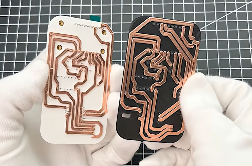
How do you make the 3D printed board conductive?
Conductivity is achieved by applying copper tape to the printed plastic board. After printing and removing any stringing, you clean the surface with isopropyl alcohol. Cut a piece of copper tape slightly larger than the board and press it firmly onto the top, covering the raised traces. Use a blunt tool (like a plastic spudger) to burnish the tape into the trace edges so it conforms to the shape. Then, using a sharp hobby knife, carefully cut the copper along the edges of each raised trace. Peel away the copper from the non-trace areas (the recessed regions). The remaining copper strips become your conductive pathways. For vias or component pads, you can puncture the tape and insert wires or solder components directly onto the copper.
What are the limitations of this method?
This technique is not production-ready and has several trade-offs. Trace widths must be very thick (≥1.5 mm) to survive cutting and peeling, so complex, high-density layouts are impractical. The copper tape provides only a thin conductor, limiting current capacity to maybe 0.5–1 A. Solder adhesion can be poor because copper tape lacks the oxide layer of true PCB copper; you may need to add flux or rough up the surface. The boards are also mechanically fragile—the plastic substrate can warp if hot components are soldered directly. Finally, the process is manual and requires careful cutting, which can be tedious for boards with many traces. Despite these drawbacks, for quick one-off prototypes of simple microcontroller circuits, it’s a viable alternative to waiting days for a fab house.

How does this compare to using a CNC mill for PCB prototyping?
CNC milling is a common alternative for rapid PCB creation, but it has its own pros and cons. Milling requires a dedicated CNC machine (often expensive) and produces boards with thicker copper (1 oz or more) that can handle higher currents. However, milling generates dust and noise, and the bit must be precisely aligned; also, milling thin traces can be challenging. The 3D printer method is arguably more accessible because many hobbyists already own a 3D printer. It’s also quieter and cleaner—no flying debris. On the downside, the copper tape approach yields lower conductivity and is less durable. For very simple, low-power circuits, the 3D printer method wins on convenience; for anything requiring reliable traces or higher current, a CNC mill or traditional etching is better.
What types of projects is this method suitable for?
This technique shines for rapid prototyping of simple microcontroller projects—think Arduino-compatible blink circuits, sensor breakouts, or small audio amplifiers. Any design with a low number of traces, wide tolerances, and low current requirements works well. It’s also great for educational settings where students need to test a circuit design quickly without waiting for fabrication. Because the board is purely mechanical, it’s easy to iterate: if a trace needs changing, just edit the 3D model and reprint. The resulting board can be used for breadboard-style testing or even as a permanent fixture in a non-critical project. However, avoid using it for high-speed signals, RF circuits, or power electronics where trace resistance and parasitic inductance matter.